- 您现在的位置:买卖IC网 > Sheet目录17359 > AD587JNZ (Analog Devices Inc)IC VREF SERIES PREC 10V 8-PDIP
AD587
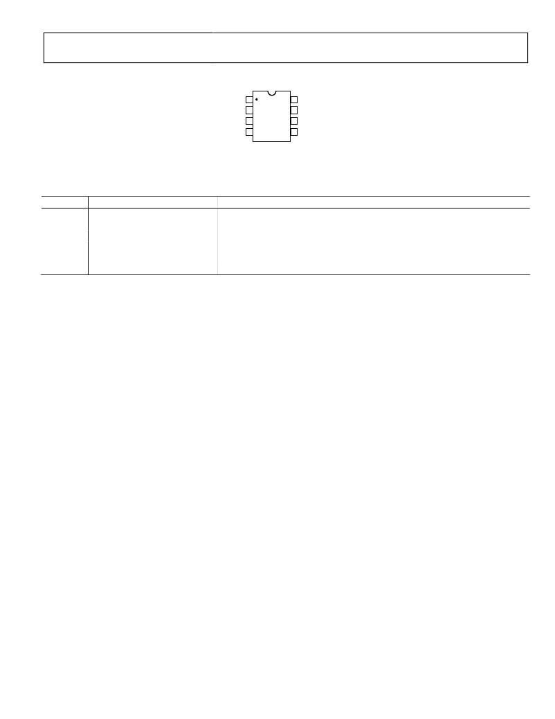
PIN CONFIGURATION AND FUNCTION DESCRIPTIONS
TP* 1
8
NOISE
REDUCTION
AD587
TP* 3 (Not to Scale) 6
+V IN 2 7
TOP VIEW
TP*
V OUT
GND 4
5
TRIM
*TP DENOTES FACTORY TEST POINT.
NO CONNECTIONS SHOULD BE MADE
TO THESE PINS.
Figure 2. Pin Configuration
Table 3. Pin Function Descriptions
Pin No.
1, 3, 7
2
4
5
6
8
Mnemonic
TP
+V IN
GND
TRIM
V OUT
NOISE REDUCTION
Description
No Connection. Leave floating.
Input Voltage.
Ground.
Output Voltage.
Noise Reduction of Output Voltage. Reduces noise via external capacitor to ground.
Rev. H | Page 5 of 12
发布紧急采购,3分钟左右您将得到回复。
相关PDF资料
RB-2409S/H
CONV DC/DC 1W 24VIN 09VOUT
ADR291GRUZ
IC VREF SERIES PREC 2.5V 8-TSSOP
ADR440ARZ
IC VREF SERIES PREC 2.048V 8SOIC
MIC2545A-2BTS
IC SW CURR LIMIT HI SIDE 14TSSOP
ADR291GT9Z
IC VREF SERIES PREC 2.5V TO-92-3
RB-2405S/H
CONV DC/DC 1W 24VIN 05VOUT
LM4050CEM3-4.1+T
IC VREF SHUNT PREC 4.096V SOT23
TH3D336M010E0800
CAP TANT 33UF 10V 20% 2917
相关代理商/技术参数
AD587JNZ1
制造商:AD 制造商全称:Analog Devices 功能描述:High Precision 10 V Reference
AD587JQ
功能描述:IC VREF SERIES PREC 10V 8-CERDIP RoHS:否 类别:集成电路 (IC) >> PMIC - 电压基准 系列:- 标准包装:2,000 系列:- 基准类型:旁路,可调节,精度 输出电压:1.24 V ~ 16 V 容差:±0.5% 温度系数:- 输入电压:1.24 V ~ 16 V 通道数:1 电流 - 阴极:100µA 电流 - 静态:- 电流 - 输出:20mA 工作温度:-40°C ~ 85°C 安装类型:通孔 封装/外壳:TO-226-3、TO-92-3(TO-226AA)成形引线 供应商设备封装:TO-92-3 包装:带卷 (TR)
AD587JR
功能描述:IC VREF SERIES PREC 10V 8-SOIC RoHS:否 类别:集成电路 (IC) >> PMIC - 电压基准 系列:- 标准包装:3,000 系列:- 基准类型:旁路,精度 输出电压:5V 容差:±0.5% 温度系数:100ppm/°C 输入电压:- 通道数:1 电流 - 阴极:80µA 电流 - 静态:- 电流 - 输出:15mA 工作温度:-40°C ~ 85°C 安装类型:表面贴装 封装/外壳:TO-236-3,SC-59,SOT-23-3 供应商设备封装:SOT-23-3 包装:带卷 (TR) 其它名称:LM4040CIM3-5.0MLTRLM4040CIM3-5.0MLTR-ND
AD587JR-REEL
功能描述:IC VREF SERIES PREC 10V 8-SOIC RoHS:否 类别:集成电路 (IC) >> PMIC - 电压基准 系列:- 标准包装:3,000 系列:- 基准类型:旁路,精度 输出电压:5V 容差:±0.5% 温度系数:100ppm/°C 输入电压:- 通道数:1 电流 - 阴极:80µA 电流 - 静态:- 电流 - 输出:15mA 工作温度:-40°C ~ 85°C 安装类型:表面贴装 封装/外壳:TO-236-3,SC-59,SOT-23-3 供应商设备封装:SOT-23-3 包装:带卷 (TR) 其它名称:LM4040CIM3-5.0MLTRLM4040CIM3-5.0MLTR-ND
AD587JR-REEL7
功能描述:IC VREF SERIES PREC 10V 8-SOIC RoHS:否 类别:集成电路 (IC) >> PMIC - 电压基准 系列:- 标准包装:3,000 系列:- 基准类型:旁路,精度 输出电压:5V 容差:±0.5% 温度系数:100ppm/°C 输入电压:- 通道数:1 电流 - 阴极:80µA 电流 - 静态:- 电流 - 输出:15mA 工作温度:-40°C ~ 85°C 安装类型:表面贴装 封装/外壳:TO-236-3,SC-59,SOT-23-3 供应商设备封装:SOT-23-3 包装:带卷 (TR) 其它名称:LM4040CIM3-5.0MLTRLM4040CIM3-5.0MLTR-ND
AD587JRZ
功能描述:IC VREF SERIES PREC 10V 8-SOIC RoHS:是 类别:集成电路 (IC) >> PMIC - 电压基准 系列:- 标准包装:3,000 系列:- 基准类型:旁路,精度 输出电压:3V 容差:±0.5% 温度系数:100ppm/°C 输入电压:- 通道数:1 电流 - 阴极:82µA 电流 - 静态:- 电流 - 输出:15mA 工作温度:-40°C ~ 85°C 安装类型:表面贴装 封装/外壳:6-TSSOP(5 引线),SC-88A,SOT-353 供应商设备封装:SC-70-5 包装:带卷 (TR) 其它名称:296-20888-2
AD587JRZ1
制造商:AD 制造商全称:Analog Devices 功能描述:High Precision 10 V Reference
AD587JRZ-REEL
功能描述:IC VREF SERIES PREC 10V 8-SOIC RoHS:是 类别:集成电路 (IC) >> PMIC - 电压基准 系列:- 标准包装:2,000 系列:- 基准类型:旁路,可调节,精度 输出电压:1.24 V ~ 16 V 容差:±0.5% 温度系数:- 输入电压:1.24 V ~ 16 V 通道数:1 电流 - 阴极:100µA 电流 - 静态:- 电流 - 输出:20mA 工作温度:-40°C ~ 85°C 安装类型:通孔 封装/外壳:TO-226-3、TO-92-3(TO-226AA)成形引线 供应商设备封装:TO-92-3 包装:带卷 (TR)
